SERVICE HOTLINE:
15861593767
SERVICE HOTLINE:15861593767
PRODUCT CLASSIFICATION:INDUSTRIALl MICROSCOPE SERIES
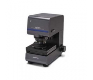
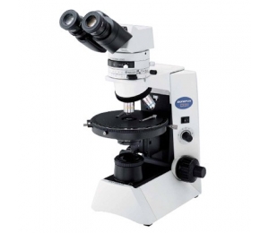
PRODUCT IABELING: desktop Vertical floor Horizontal Optical projection projector optical projection horizontal Floor inverted Metallographic microscope Stereo microscope
Number of people concerned:already existing373Customer focus
Share quickly:
CONSULT IMMEDIATELY
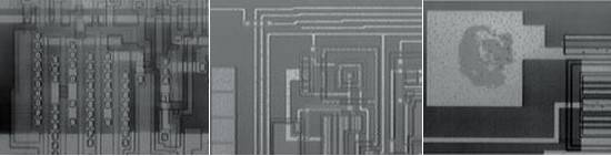
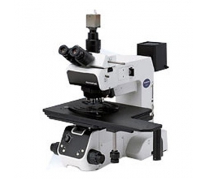
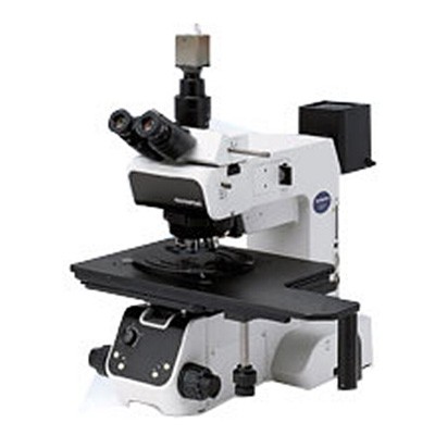
1. With the development of electronic equipment miniaturization and ultra-thin, the packaging technology of semiconductor devices is also evolving rapidly. Using Olympus near infrared microscope, we can carry out non-destructive inspection and Analysis on SIP (system in package), 3D assembly, CSP (chip size package) and other areas that can not be seen by visual observation.
2. Mx-ir / bx-ir is a kind of transparent infrared microscope. It is suitable for non-destructive inspection of CSP / SIP in package chip and wafer level.
3. In flip chip soldering, the soldered parts and modules after assembly cannot be inspected by visible light. However, if a near-infrared microscope is used, the interior of the IC chip can be observed through the silicon without damaging the package. As long as it is placed under the microscope, it is easy to analyze the bad condition. It is also valid to specify the processing location that must be FIB (focused ion beam).
4. The change of device caused by high temperature and high humidity test of wafer level CSP can be checked by non-contact method. In addition, it can reliably observe the leakage caused by the melting and corrosion of the copper lead and the peeling of the resin part.
5. For MX series products, large samples such as 150-300 mm wafers should be observed.
6. BX series products should be observed under 100 mm and small samples.
7. Bxfm series products should be small-scale design and online observation of embedded devices.
Contact person: general manager you
Contact: 15861593767
website:http://www.novatech-cn.com/
Address: room 313-319, building B, innovation and Creative Industry Park, No.5 Xinhua Road, Xinwu District, Wuxi