SERVICE HOTLINE:
15861593767
SERVICE HOTLINE:15861593767
PRODUCT CLASSIFICATION:CUSTOMIZED MICROSCOPE SERIES
PRODUCT IABELING: desktop Vertical floor Horizontal Optical projection projector optical projection horizontal Floor inverted Metallographic microscope Stereo microscope
Number of people concerned:already existing382Customer focus
Share quickly:
CONSULT IMMEDIATELY
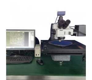
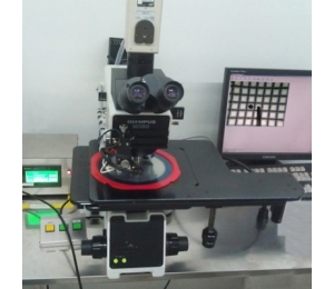
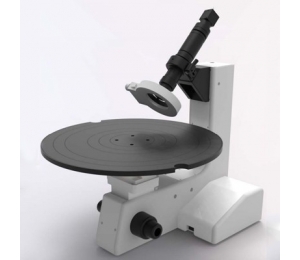
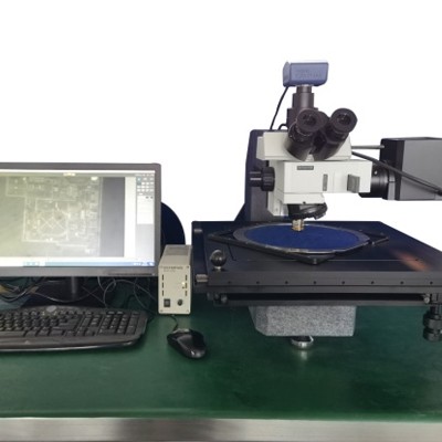
Application:
Observe the inside of wafer and compound semiconductor;
Observe the inside of the package chip and CSP bump.
characteristic:
1. It can be used for field and near infrared observation;
2. Nondestructive observation;
3. The infrared optical system of Olympus is adopted;
From 4.5 times to 100 times infrared lens, Olympus unique aberration correction technology is adopted from visible wavelength to near infrared;
5. Clear near infrared imaging and simple measurement are realized by using the unique low illumination sensitive camera of Jena, Germany;
6. The solid marble machine provides stable and reliable image quality;
7. The size of the stage can be customized according to the sample size
Contact person: general manager you
Contact: 15861593767
website:http://www.novatech-cn.com/
Address: room 313-319, building B, innovation and Creative Industry Park, No.5 Xinhua Road, Xinwu District, Wuxi